


Servicios Personalizados
Revista
Articulo
 Inglés (pdf)
 Articulo en XML
 Referencias del artículo
 Enviar articulo por email
Indicadores
-
 Citado por SciELO
 -
 Accesos
Links relacionados
-
 Similares en
SciELO
Similares en
SciELO
Compartir

 Permalink
Acta Nova
versión On-line ISSN 1683-0789
RevActaNova. vol.3 no.1 Cochabamba dic. 2005
Artículo Científico
Nd3+ and Er3+ in morphous silicon compounds for photonics
Daniel Biggemann
Instituto de Física "Gleb Wataghin", UNICAMP, 13083-970 Campinas, SP, Brazil
Telefono: +55 19 3788 5396
Fax: +55 19 3788 5376
Email: bigge@ifi.unicamp.br
Abstract
This work presents a study of the photoluminescence (PL) of Nd and Er-doped hydrogenated amorphous silicon compounds. Thin films were deposited by rf sputtering a silicon target partially covered by small metallic Nd or Er platelets in a H2 + N2 + Ar or H2 + O2 + Ar atmosphere, respectively. PL measurements on waveguide geometry were performed. The experimental results indicate a super linear behavior of the PL with excitation power for both materials at 10 K. There were found cavity modes indicating a interference process inside the waveguide. The results suggest the presence of stimulated emission process and the power of the materials to be used for photonic purposes.
Key Words: Neodymium, erbium, amorphous silicon, photoluminescence, photonics.
The high demand for speed of high quantity information transfer requires nowadays faster devices. Changing electrons by photons and copper wires by optical fibers the challenges are easier to be reached. Optical fibers offer the possibility to transmit information through a wide band with multiple signals without interference. Nevertheless the microelectronics world, where all the information is need to be processed, is constructed on silicon-based technology. Unfortunately all the present photonic devices are developed with materials such as InP or GaAs because the silicon's indirect bandgap turns it a bad light emitter. This fact has motivated a lot of research in new silicon-based materials as efficient light sources [2, 6].
An interesting way to circumvent this lack of silicon as light emitter without breaking the microelectronics compatibility is using rare earth (RE) ions as dopants in different silicon-based materials.
These ions are characteristic to emit light due to internal electronic transitions between incomplete 4f states. These transitions are electric dipole forbidden but they become to be allowed when the RE ions occupy non center-symmetric sites inside the host. [4, 3] That is why, for example, Er3+ ions have stronger luminescence in amorphous rather than in crystalline silicon. Two REs ions particularly interesting are Er3+ and Nd3+. The Er3+ luminescence in the near infrared region at ~ 1.54 μm due to 4I13/2→ 4I15/2 transition coincides with the lowest absorption region of commercial silica-based optical fibers.[8] Although the Nd3+ emission does not coincide with any of optical fibers' low absorption window, this ion is the most popular RE ion used for solid state lasers as active medium. [7] The luminescence lines of Nd3+ ions lie in the near infrared region at ~ 890, ~ 1100 and ~ 1370 nm, which are due to transitions 4I3/2 → 4I9/2 , 4I3/2 → 4I11/2 and 4I3/2 → 4I13/2, respectively.
An interesting way to study silicon based materials doped with Er or Nd are amorphous silicon (a-Si) thin films. This amorphous material allows higher REs' concentrations than its crystalline counterpart. During the preparation the samples can be alloyed with other element such as O, N or C which are used to modify the optical parameters. These optical parameters (index of refraction and optical bandgap) are controlled in order to enhance the RE luminescence. In this paper is reported a study of the photoluminescence (PL) of hydrogenated amorphous silicon sub-nitrides (a SiNx : H) and sub-oxides (a-SiOx : H) doped with Nd and Er, respectively. ~ 0.5 um thick films were deposited on Si <100> 89 μm thick substrates by rf co-sputtering technique from a 99.999% purity Si target partially covered by 99.9% pure small metallic RE platelets. Depending on the RE, an high purity H2 + N2 + Ar (for Nd) or H2 + O2 + Ar (for Er) gas mixture was added during the deposition.
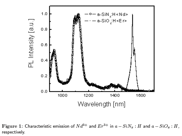
There were performed PL measurements exciting the samples with all lines of a CW Ar+ laser at different excitation intensities. PL spectra were acquired at different temperatures (from 10 to 300 K). The signal was dispersed by a 30 cm spectrograph and detected by a thermo-electrically cooled 512 element InGaAs diode array. Typical PL spectra of a SiNx : H < Nd > and a SiOx : H < Er > are shown in Figure 1.
There were performed lifetime measurements and PL emission intensity as a function of excitation power in samples with waveguide geometry;[9] i.e. detecting the signal at a cleaved face of the substrate. PL measurements at 10 K as a function of power excitation in waveguide geometry are shown in Figure 2. These spectra show a super linear growth of PL.

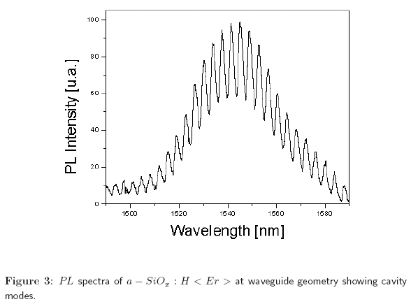
The behavior of the PL intensity with the excitation power suggest for both materials that more than one photon is emitted by excited ion. On the other hand, lifetime measurements in a SiNx : H < Nd > (not shown) show a diminution of lifetime when the excitation power increases. This decrease is characteristic of the onset of stimulated emission. Cavity modes (see Figure 3) were also found in a SiOx : H < Er > emission.
All of these results strongly suggest the power of a SiNx : H < Nd > and a SiOx : H < Er > for photonic purposes as integrated-compatible optical amplifiers.
The main challenge is to optimize the materials to have all these characteristics present at 10 K at room temperature too.
The author acknowledges the Brazilian agencies FAPESP and CAPES for financial support and Prof. L. Tessler for important discussions.
References
[1] D. Biggemann and L. R. Tessler. Sci. Eng. B. 2003, 105, 188-190. [2] Canham. L. Nature 2000. 408, 411-412.
[3] S. Hüfner. Optical Spectra of Transparent Rare Earth Compounds. Academic Press, New York, 1978. [ Links ]
[4] B. R. Judd. Phys. Rev. 1962, 127, 750-761.
[5] M.Castagna ;S.Coffa ; M.Monaco ; A.Muscara ;L. Caristia ;S. Lorenti and Messina. A. Mater. Sci. and Eng. B 2003, 105, 83-90.
[6] Opt. Mater. Si-based Photonics: Towards True Monolithic Integration. 2005, 27.
[7] Millenia. of Spectra Physics (10 W CW at 532 nm) and Verdi, of Coherent (10W CW at 532 nm). [ Links ]
[8] S. M. Sze. Physics of Semiconductor Devices. John Wiley and Sons, New York, 1981. [ Links ]
[9] L. R. Tessler and D. Biggemann. Opt. Mater. 2005, 27, 773-775.

